
QSPI Introduction(Sample STM32)
QSPI Introduction
QSPI stands for Queued Serial Peripheral Interface, an extension of the SPI interface introduced by Motorola. QSPI has wider applications than SPI due to the enhanced functionality provided by Motorola, including the addition of a queued transmission mechanism. This led to the development of the Queued Serial Peripheral Interface Protocol (QSPI protocol) based on the SPI protocol. Here, we will focus on explaining QSPI in relation to SPI flash memory.

Using QSPI(Flash)
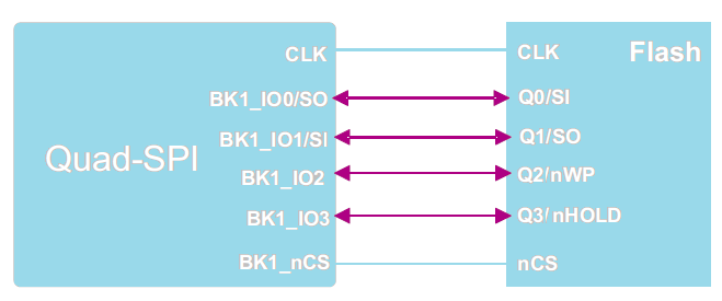
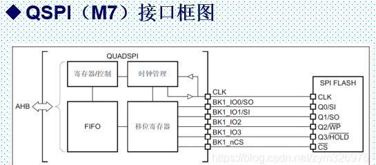
QSPI uses 6 I/Os to connect with Flash memory, including four data lines BK1_IO0~BK1_IO3, one CLK line, and one chip select output (active low) BK1_nCS. Their functions are described below:
- BK1_nCS: Chip select output (active low), used for Flash 1. If QSPI is always working in dual-quad mode, it can also be used as device select signal line for Flash 2. QSPI communication starts with the BK1_nCS line being pulled low and ends with the BK1_nCS line being pulled high.
- CLK:Clock output, used for data synchronization between QSPI and memory devices. It is generated by the communication master and determines the communication rate. The maximum clock frequency supported by different devices is not the same. For example, the maximum QSPI clock frequency of STM32 is fpclk/2. When communicating between two devices, the communication speed is limited by the slower device.
- BK1_IO0: In dual-quad/four-wire mode, it is a bidirectional I/O, and in single-wire mode, it is a serial output, used for Flash 1.
- BK1_IO1:In dual-quad/four-wire mode, it is a bidirectional I/O, and in single-wire mode, it is a serial input, used for Flash 1.
- BK1_IO2:In four-wire mode, it is a bidirectional I/O, used for Flash 1.
- BK1_IO3:In four-wire mode, it is a bidirectional I/O, used for Flash 1.
QSPI Command Sequence
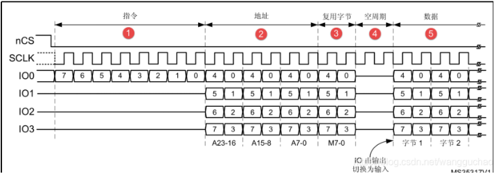
1. Instruction phase
An 8-bit instruction configured in the INSTRUCTION field of the QUADSPI_CCR[7:0] register is sent to the Flash, specifying the type of operation to be performed. Although most Flash can only receive instructions through the IO0/SO signal (single-line SPI mode) in a one-bit manner, the instruction phase can choose to send 2 bits at a time (via IO0/IO1 in dual-line SPI mode) or 4 bits at a time (via IO0/IO1/IO2/IO3 in quad-SPI mode). This can be configured through the IMODE[1:0] field in the QUADSPI_CCR[9:8] register. If IMODE = 00, the instruction phase is skipped and the command sequence starts from the address phase (if present).
2. Address Phase
In the address phase, 1-4 bytes are sent to the Flash to indicate the operation address. The number of address bytes to be sent is configured in the ADSIZE[1:0] field of the QUADSPI_CCR[13:12] register. In indirect and automatic polling modes, the address bytes to be sent are specified in the ADDRESS[31:0] field of the QUADSPI_AR register. In memory-mapped mode, the address is directly provided through the AHB (from Cortex® or DMA). The address phase can send 1, 2, or 4 bits at a time (through SO in single-line SPI mode, through IO0/IO1 in dual-line SPI mode, or through IO0/IO1/IO2/IO3 in quad-line SPI mode). This can be configured in the ADMODE[1:0] field of the QUADSPI_CCR[11:10] register. If ADMODE = 00, the address phase is skipped and the command sequence goes directly to the next phase (if it exists).
3. Alternate Bytes Phase
In the Alternate Bytes phase, 1-4 bytes are sent to the flash, typically used to control the operation mode. The number of bytes to be sent in this phase is configured in the ABSIZE[1:0] field of the QUADSPI_CCR[17:16] register. The bytes to be sent are specified in the QUADSPI_ABR register. The number of alternate bytes to be sent can be 1 bit (through SO in single-line SPI mode), 2 bits (through IO0/IO1 in dual-line SPI mode), or 4 bits (through IO0/IO1/IO2/IO3 in quad-line SPI mode). This can be configured through the ABMODE[1:0] field in the QUADSPI_CCR[15:14] register. If ABMODE = 00, the Alternate Bytes phase is skipped and the command sequence enters the next phase (if it exists) directly.
In the Alternate Bytes phase, there is a case where only a half-byte needs to be sent instead of a full byte, for example, when using the dual-line mode and sending alternate bytes in only two cycles. In this case, the firmware can use quad-line mode (ABMODE = 11) and send one byte, where bit 7 and 3 of ALTERNATE are set to “1” (IO3 remains high) and bits 6 and 2 are set to “0” (IO2 remains low). The high 2 bits of the half-byte are stored in bits 4:3 of ALTERNATE, and the low 2 bits are stored in bits 1 and 0. For example, if half-byte 2 (0010) is sent through IO0/IO1, then ALTERNATE should be set to 0x8A (1000_1010).
4.Dummy cycle phase
In the dummy cycle phase, no data is sent or received within a given 1-31 clock cycles, which is intended to allow enough time for preparing the data phase when a higher CLK frequency is used. The number of cycles specified in this phase is indicated in the DCYC[4:0] field of the QUADSPI_CCR[22:18] register. In SDR and DDR modes, the duration is specified as a certain number of full clock cycles. If DCYC is zero, the dummy cycle phase is skipped and the command sequence goes directly to the data phase (if it exists). The operating mode of the dummy cycle phase is determined by DMODE. To ensure sufficient “turnaround” time for the data signal to transition from output mode to input mode, at least one dummy cycle needs to be specified when receiving data from the Flash in dual and quad wire modes
5. Data Phase
In the data phase, any number of bytes can be sent to or received from the Flash. In indirect mode and auto-polling mode, the number of bytes to be sent/received is specified in the QUADSPI_DLR register. In indirect write mode, the data to be sent to the Flash must be written to the QUADSPI_DR register. In indirect read mode, the data received from the Flash is obtained by reading the QUADSPI_DR register. In memory-mapped mode, the read data is directly sent back to the Cortex or DMA via AHB. The data phase can send/receive 1 bit (via SO) in single-line SPI mode, 2 bits (via IO0/IO1) in dual-line SPI mode, or 4 bits (via IO0/IO1/IO2/IO3) in quad-line SPI mode. This can be configured through the ABMODE[1:0] field in the QUADSPI_CCR[15:14] register. If DMODE = 00, the data phase is skipped and the command sequence is completed immediately when nCS is pulled high. This configuration is only available for indirect write mode.
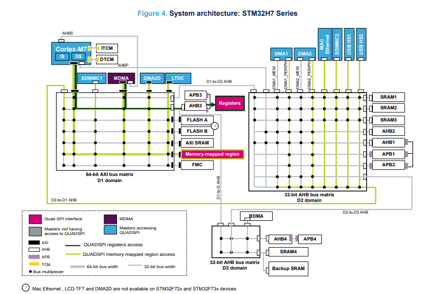
QUADSPI in a smart architecture
When using QSPI, please refer to the Application note-AN4760 and confirm the domains on page 6 to avoid any usage issues. Considering that H7 is more complex, there are three domains.

When connecting an LCD using QSPI, external Flash is used for expansion