Routing a Power Inverter Design Guidelines
Preface
The customer often encounters layout issues in motor control design, many of which are related to structural know-how. ST provides essential design guidance to help avoid common pitfalls in motor control, which can lead to excessive noise in the ADC feedback circuit that interferes with actual motor control. Additionally, we provide guidelines on MOS design to help the customer understand key points for subsequent designs.
Circuit loops Guidelines
The most important point is to avoid large loop area designs.(Avoid big area loops as much as possible!)
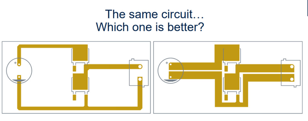
- Loops on the PCB are acting as coils
- The bigger loop area, the bigger issue
- Circuit with bigger area loop:
- Generates noise (e. g. switching of the transistors)
- Absorb noise (e. g. shunt signal feedback)
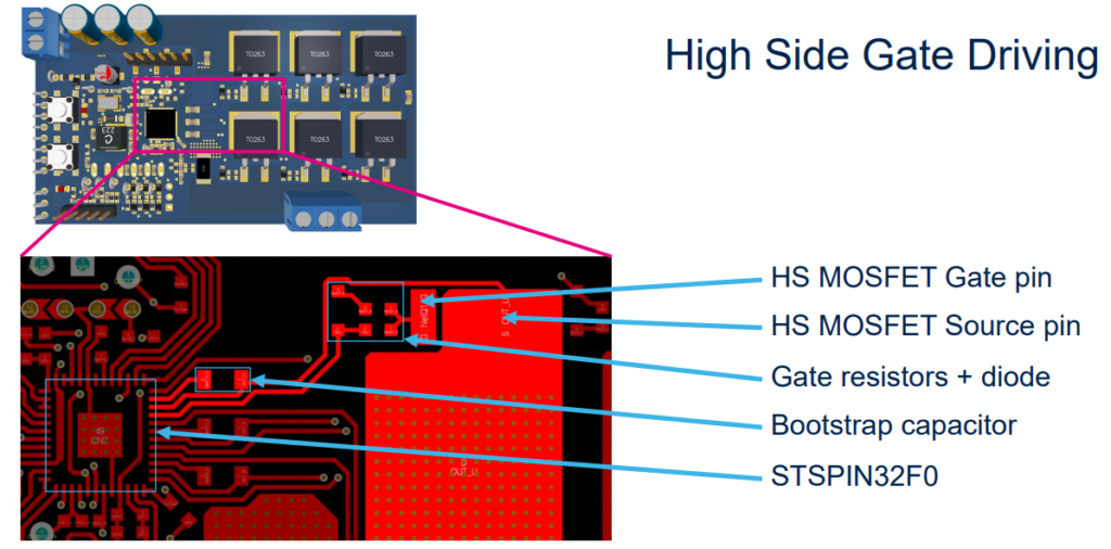
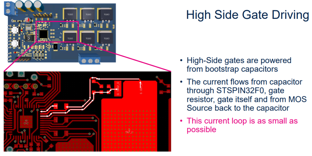
- Focus on complete loop: from source to load and
back to the source - Keep the area of the loops as small as possible!
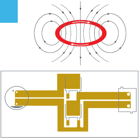
Good component placement is the key
- By optimal components placement the routing
- can be easier
- Study the schematic first and decide what blocks
should be close to each other - There is no ideal placement!
Always compromise between general rules,
specifics of the inverter, manufacturing limits, etc.
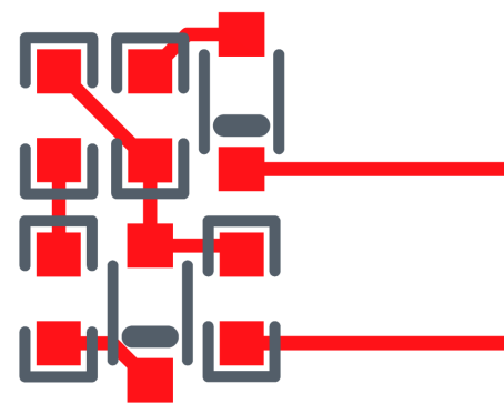
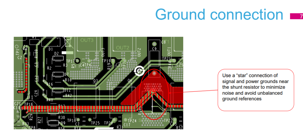
I recommend using the following connection method. Kelvin connection/Star Connection
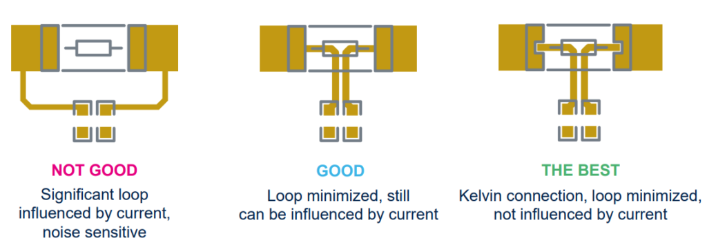
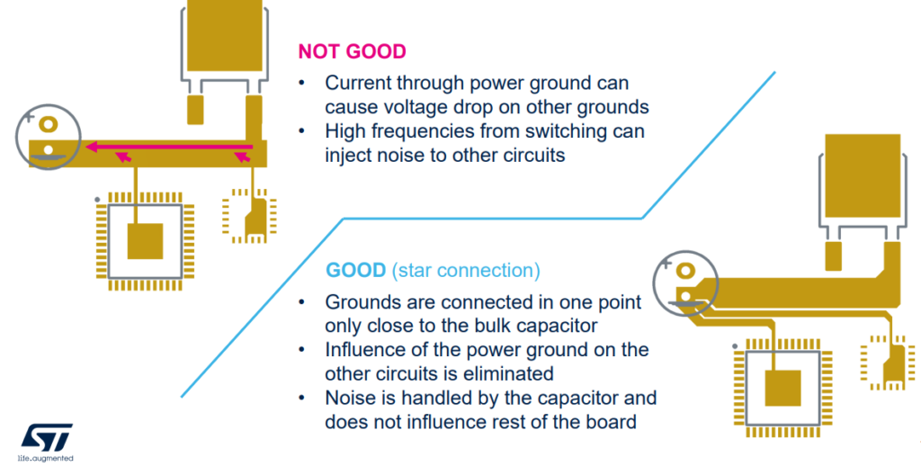
Example
Current loop area is minimized and there are no sensitive circuits inside it
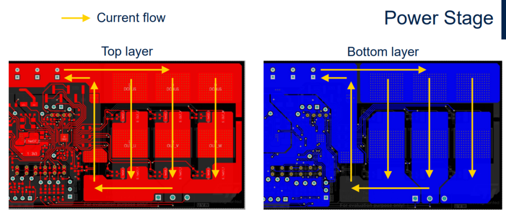
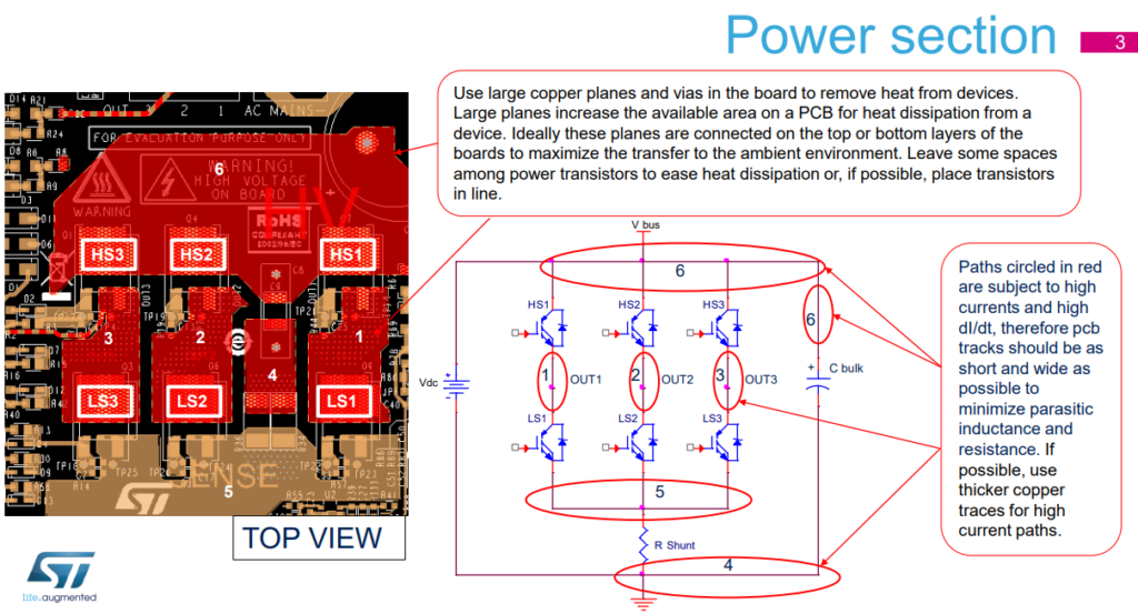

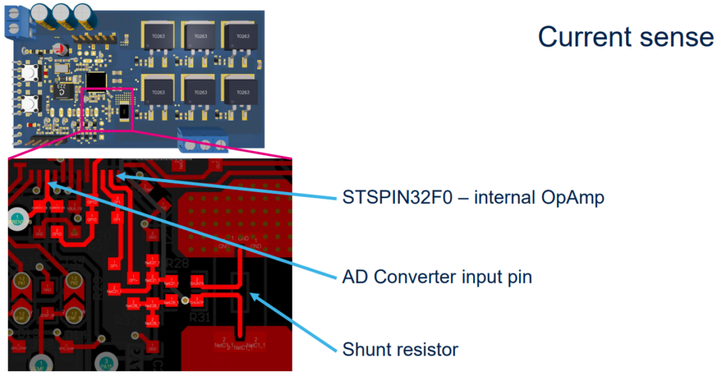
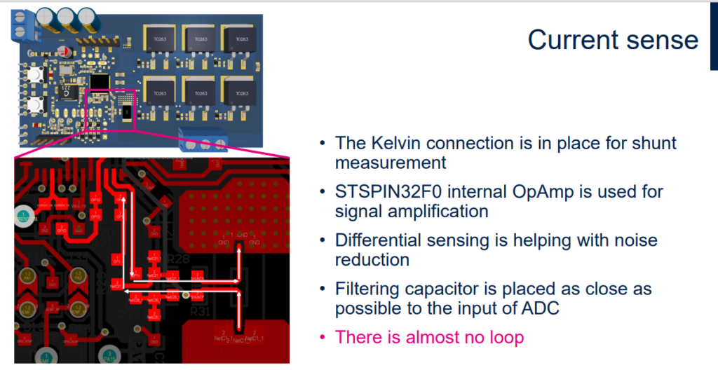
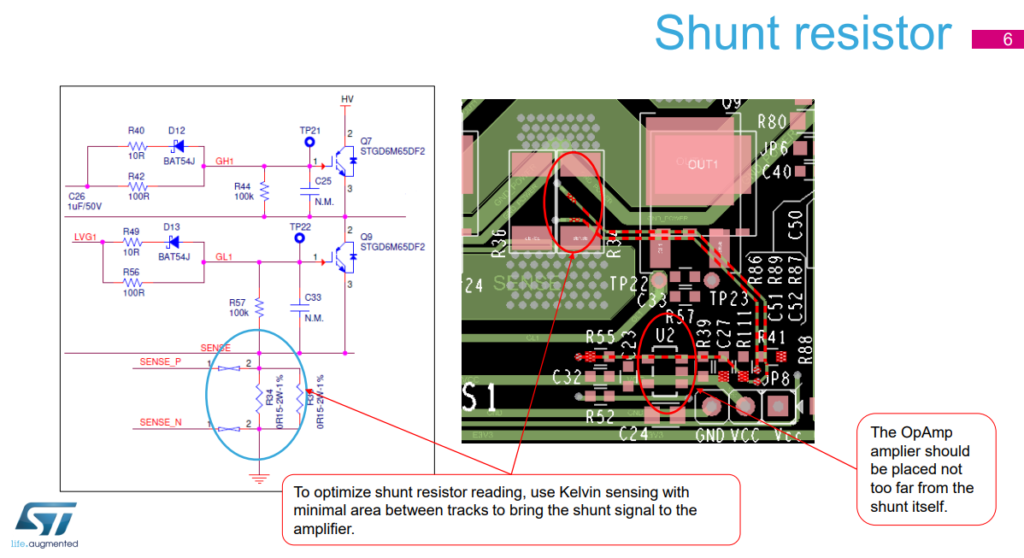
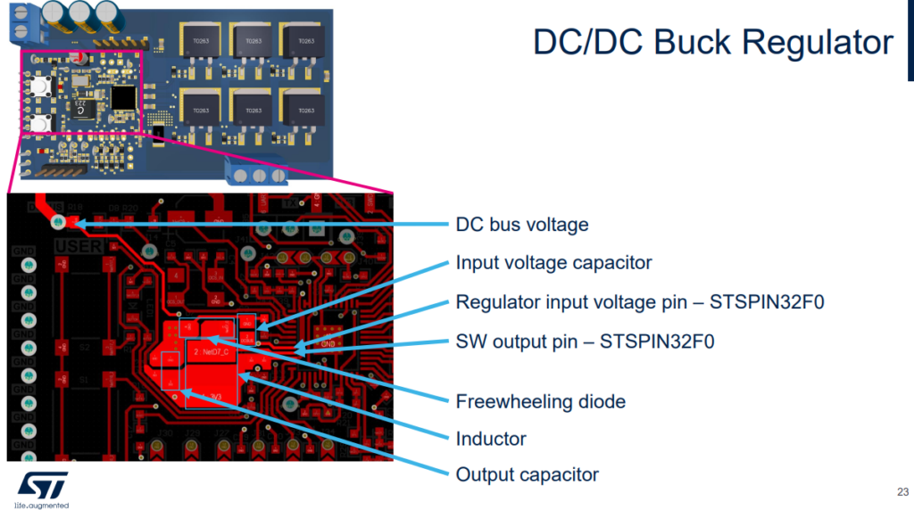

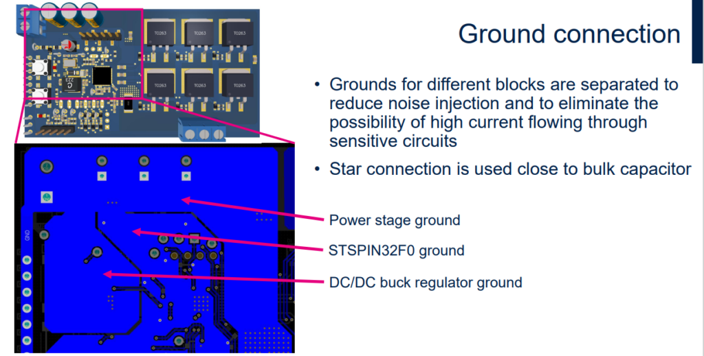
For the GND design, it is recommended to separate Digital GND and Power GND.
For other MOS design considerations, please refer to the following document: Power MOSFETs: Best Choice Guide for VRM Applications.
