Serial Peripheral Interface Bus(SPI)
Catalogue
- Preface
- 一、Introduction to SPI Protocol
- SPI Physical Layer
- SPI Protocol Layer
- Basic Communication Procedure
- Communication Interception and Stop Signals
- Data Validity
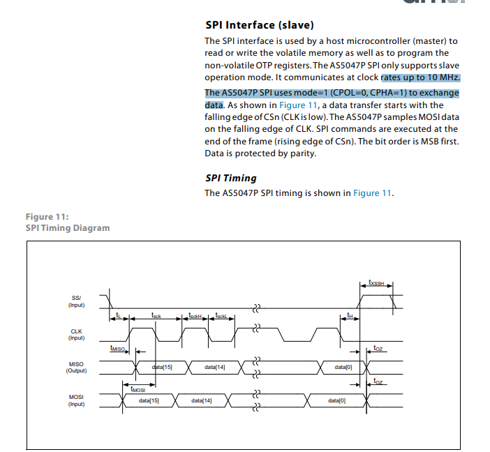
- CPOL/CPHA and Communication Modes
- 二、STM32cubeMXConfiguration
- 三、SPI in STM32 HAL Library
- SPI Initialization Structure
Introduction to SPI Protocol
The SPI protocol is a communication protocol (Serial Peripheral Interface) proposed by Motorola. It is a full-duplex communication protocol with high-speed communication on the peripheral device side. It is widely used between communication devices and MCUs, such as ADCs, LCDs, etc. The three lines of the protocol are SCK, MOSI, and MISO, and SS is used for triggering selection
SPI Physical Layer

- SS(Slave Select) SS :The SPI protocol is a communication protocol proposed by Motorola (Serial Peripheral Interface), which is a high-speed full-duplex communication protocol used extensively between communication devices and MCUs. It is widely used between devices such as ADCs, LCDs, and MCUs, with three total lines: SCK, MOSI, and MISO, and the trigger selection uses SS (Slave Select) or NSS (Chip Select) which is commonly known as the device selection signal line. When multiple SPI slave devices are connected to the SPI host, the selection of the device is controlled by other signal lines. Each SPI device uses these three lines for communication, including the MISO line on the slave device itself. The number of signal lines on the NSS of the slave device determines the number of devices that can be addressed using this protocol. If there is no device address, the NSS signal line is used for detection. When the host wants to select a slave device, the signal line of that slave device is set to low, indicating that it is selected, and communication with that device begins. Therefore, the NSS line is set low to trigger the slave to receive signals from the master or to request data from the slave, similar to the address concept in I2C
- SCK(Serial Clock):the clock signal line used for data synchronization during communication, generated by the communication host device, and determines the communication frequency. Different devices support different maximum frequencies, such as the STM32 SPI clock frequency with a maximum of fpclk/2. When communicating between two devices, the communication speed is determined by the SCK frequency.
- MOSI (Master Output, Slave Input): the output line of the master device, which sends data to the slave device. The direction of this line is from the master to the slave.
- MISO (Master Input, Slave Output): the input line of the master device, which receives data from the slave device. The direction of this line is from the slave to the master.
二、SPI Protocol Layer
一、Basic Communication Procedure

Both the machine and signal source of SPI come from the master device. NSS, SCK, and MOSI are generated by the master device, while MISO is generated by the slave device. The slave device’s signal is read through the signal line. MOSI (SS) is effective only during rare MISO time slots, and is used to transfer short-term data.
CPOL/CPHA and Communication Modes
In summary, the SPI protocol is a communication protocol used between devices and MCUs, using three lines: SCK, MOSI, and MISO, with trigger selection using SS or NSS. The clock signal is generated by the host device, and the data transmission direction depends on whether it is a master or slave device.
- CKPOL = CPOL = POL = Polarity = Clock
- CKPHA= CPHA = PHA = Phase = Clock phase
- SCK=SCLK=SPI clock
- Edge, the moment that is always used, refers to the rising or falling edge (falling edge) cycle, which has two edges, called:
- Leading edge = previous edge = first edge, when the starting voltage is 1, it is the time when 1 becomes 0, and when the starting voltage is 0, it is the time when 0 becomes 1;
- Trailing edge = next edge = second edge, when the starting voltage is 1, it is the time when it starts to become 1 (which may occur after the first 1 becomes 0), and when the starting voltage is 0, it is the time when 1 becomes 0;

PS:This CPOL/CP needs to be standardized or referred to the correct use of sensors and other products in the HA for communication interchangeability.
Taking AS5047P as an example,

there are explicit capabilities.
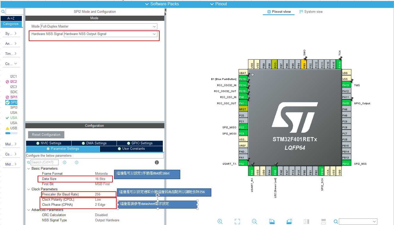
三、STM32cubeMXConfiguration

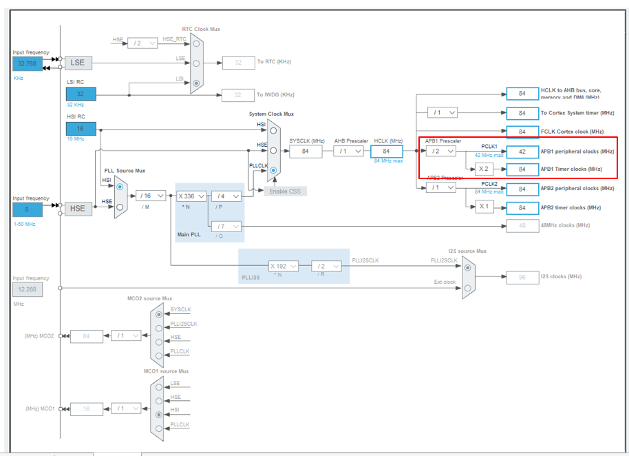
So, due to this reason, the figure below uses 1, which can be used to replace the previous figure that uses 84MHz, to use the SPI CLK at a speed of 284/256MHz.

四、SPI in STM32 HAL Library
SPI Initialization Structure
Similarly to other peripherals, the STM32 HAL library provides SPI initialization structures and initialization functions to configure the SPI peripheral. The initialization structures are defined in the library files.
STM32F4xx_hal_spi.hSTM32F4xx_hal_spi.c
The initialization structures are defined in the library files from STM32CubeMX
static void MX_SPI2_Init(void)
{

/* USER CODE BEGIN SPI2_Init 0 */

/* USER CODE END SPI2_Init 0 */

/* USER CODE BEGIN SPI2_Init 1 */

/* USER CODE END SPI2_Init 1 */
/* SPI2 parameter configuration*/
hspi2.Instance = SPI2;//這邊是選用SPI2
hspi2.Init.Mode = SPI_MODE_MASTER;/*設定SPI 的主/從機端模式*/
hspi2.Init.Direction = SPI_DIRECTION_2LINES;
hspi2.Init.DataSize = SPI_DATASIZE_16BIT;*設定SPI 的資料幀長度,可選8/16 位*/
hspi2.Init.CLKPolarity = SPI_POLARITY_LOW;
hspi2.Init.CLKPhase = SPI_PHASE_2EDGE;
hspi2.Init.NSS = SPI_NSS_HARD_OUTPUT;//這邊看需求設定可用內建
hspi2.Init.BaudRatePrescaler = SPI_BAUDRATEPRESCALER_256;//這個是直接關西到傳輸速度
hspi2.Init.FirstBit = SPI_FIRSTBIT_MSB;
hspi2.Init.TIMode = SPI_TIMODE_DISABLE;
hspi2.Init.CRCCalculation = SPI_CRCCALCULATION_DISABLE;
hspi2.Init.CRCPolynomial = 10;
if (HAL_SPI_Init(&hspi2) != HAL_OK)
{
Error_Handler();
}
/* USER CODE BEGIN SPI2_Init 2 */

/* USER CODE END SPI2_Init 2 */

}
2.Function
HAL_StatusTypeDef HAL_SPI_Transmit(SPI_HandleTypeDef *hspi, uint8_t *pData, uint16_t Size, uint32_t Timeout);

HAL_StatusTypeDef HAL_SPI_Receive(SPI_HandleTypeDef *hspi, uint8_t *pData, uint16_t Size, uint32_t Timeout);

HAL_StatusTypeDef HAL_SPI_TransmitReceive(SPI_HandleTypeDef *hspi, uint8_t *pTxData, uint8_t *pRxData, uint16_t Size, uint32_t Timeout);

HAL_StatusTypeDef HAL_SPI_Transmit_IT(SPI_HandleTypeDef *hspi, uint8_t *pData, uint16_t Size);

HAL_StatusTypeDef HAL_SPI_Receive_IT(SPI_HandleTypeDef *hspi, uint8_t *pData, uint16_t Size);

HAL_StatusTypeDef HAL_SPI_TransmitReceive_IT(SPI_HandleTypeDef *hspi, uint8_t *pTxData, uint8_t *pRxData, uint16_t Size);

HAL_StatusTypeDef HAL_SPI_Transmit_DMA(SPI_HandleTypeDef *hspi, uint8_t *pData, uint16_t Size);

HAL_StatusTypeDef HAL_SPI_Receive_DMA(SPI_HandleTypeDef *hspi, uint8_t *pData, uint16_t Size);

HAL_StatusTypeDef HAL_SPI_TransmitReceive_DMA(SPI_HandleTypeDef *hspi, uint8_t *pTxData, uint8_t *pRxData, uint16_t Size);

HAL_StatusTypeDef HAL_SPI_DMAPause(SPI_HandleTypeDef *hspi);

HAL_StatusTypeDef HAL_SPI_DMAResume(SPI_HandleTypeDef *hspi);

HAL_StatusTypeDef HAL_SPI_DMAStop(SPI_HandleTypeDef *hspi);
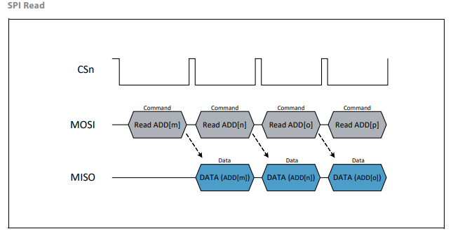
PS:If you need to receive data from the AS5047P sensor and view it as a packet, starting from the second byte received, you can set the size to 2 when using TransmitReceive.

SPI_DMA Sample code
It is recommended to add CS pin high or low signal to achieve message synchronization in the HAL_SPI_TransmitReceive_DMA function, right after the “Enable the SPI Error Interrupt Bit” comment.
HAL_StatusTypeDef HAL_SPI_TransmitReceive_DMA(SPI_HandleTypeDef *hspi, uint8_t *pTxData, uint8_t *pRxData,uint16_t Size)

******************以上省略***********
  /* Enable the SPI Error Interrupt Bit */
  __HAL_SPI_ENABLE_IT(hspi, (SPI_IT_ERR));
HAL_GPIO_WritePin(GPIOA, GPIO_PIN_15, GPIO_PIN_RESET);
  /* Enable Tx DMA Request */
  SET_BIT(hspi->Instance->CR2, SPI_CR2_TXDMAEN);

error :
  /* Process Unlocked */
  __HAL_UNLOCK(hspi);
  return errorcode;
In the callback function, you can raise the pin signal.
void HAL_SPI_TxCpltCallback(SPI_HandleTypeDef *hspi)
{
	HAL_GPIO_WritePin(GPIOA, GPIO_PIN_10, GPIO_PIN_SET);
}

void HAL_SPI_TxRxCpltCallback(SPI_HandleTypeDef *hspi)
{
	HAL_GPIO_WritePin(GPIOA, GPIO_PIN_10, GPIO_PIN_SET);
}
